Introduction

Numbering Systems
Binary and Hexadecimal Numbers
A -bit binary number ranges from .
To convert a decimal to a binary number, repeatedly divide by 2. The remainder goes in the next most significant bit.

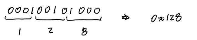
For binary to hexadecimal conversion, group bits into nibbles (4 bits), and then convert to a single hex digit.
Signed Numbers
Signed digit
- Direct addition doesn't work
- Both 1000 and 0000 represent 0
- The range is
Two's complement
- Direct addition works
- 0000 is the only representation of 0
- The range is .
The two's complement of a number is -x = ~x + 1
- Start from the LSB and copy all bits up to and including the first 1
- Invert all remaining bits

| Number | Two's complement |
|---|---|
| 127 | 01111111 |
| 1 | 00000001 |
| 0 | 00000000 |
| -1 | 11111111 |
| -128 | 10000000 |

Signed Arithmetic
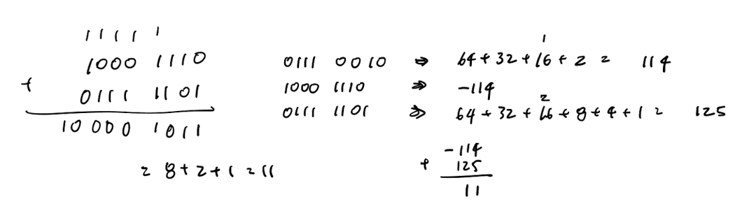
Addition:
- Directly add the numbers together
- Check for overflow
Note that adding a positive number with a negative number cannot result in overflow. You can just drop the additional bits.
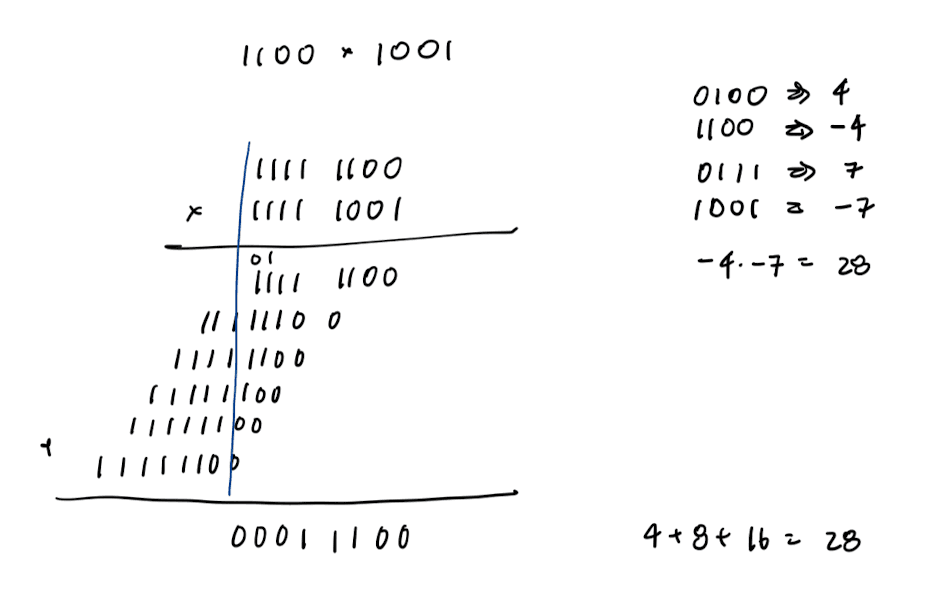
Multiplication:
- Sign-extend both numbers to the product bit width
- Multiply as if they were unsigned
- Discard overflowed bits
Sign-extension involves copying the MSB into the new bits. The product bit width of two n-bit numbers is 2n.
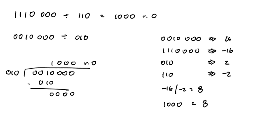
Division:
- Convert the numbers to positive
- Perform division
- Convert the quotient to the appropriate sign
- Convert the remainder to take the sign of the number being divided
Digital Logic Gates
Multiple-Input Logic Gates
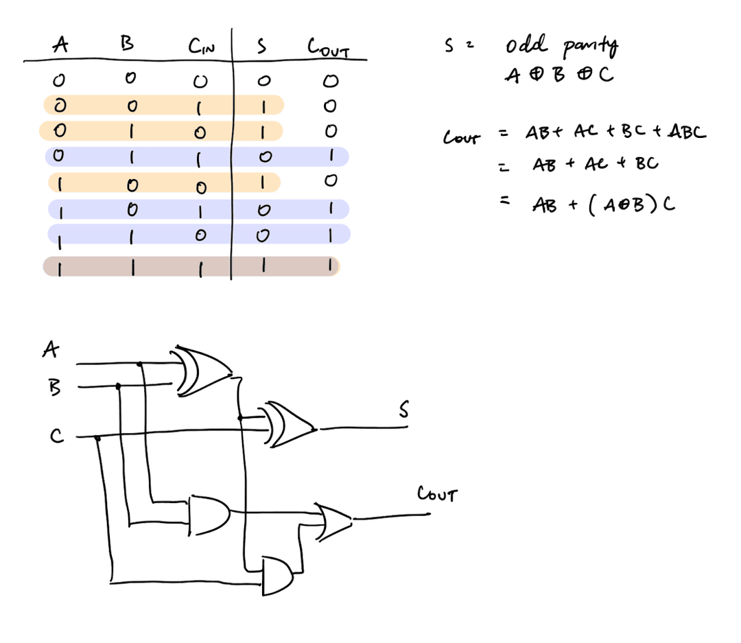
Multi-input XNOR gate returns whether there is even parity. In the two-input case, it is the same as an equality gate. Multi-input XOR returns whether there is odd parity.
Adders
1-bit adders take in three bits (A, B, Cin) and output two bits (S and Cout).
The ripple carry adder chains 1-bit adders together and carries the carry out to the next adder. This is a ripple carry adder that has been repurposed to subtract from :

Ring Oscillators
Ring oscillators are made from an odd number of inverters connected in a ring. The signal keeps inverting as it propagates around the ring, creating an oscillation.
The oscillation frequency is , where is the number of inverters and is the propagation delay of each inverter.

Transistors
Logic gates are built from transistors, which are like voltage-controlled switches. Two ports get connected depending on the voltage of the third.
nMos transistors are connected when the gate voltage is high, and pMos transistors are connected when the gate voltage is low.

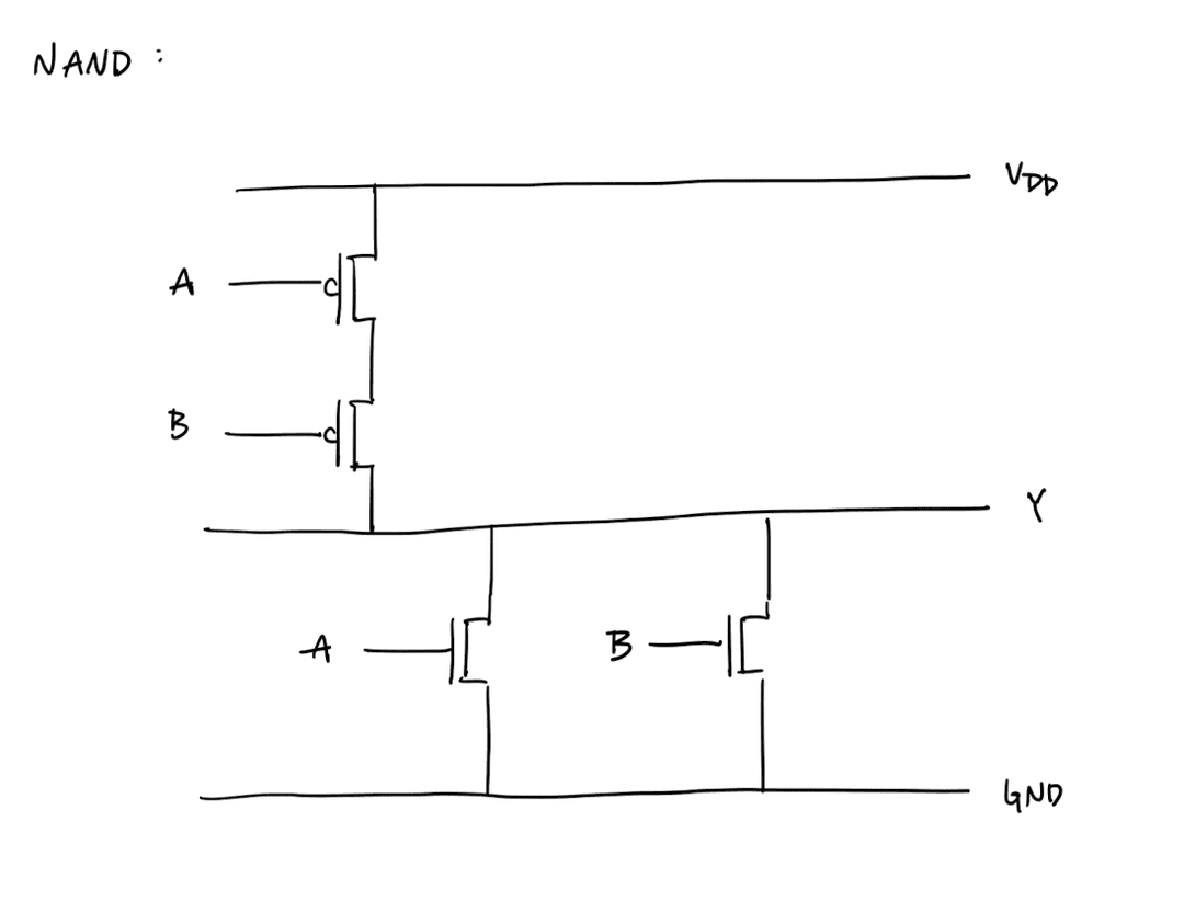
nMOS transistors pass good 0s, so they should be connected to ground. pMOS transistors pass good 1s, so they should be connected to VDD.
CMOS uses both nMOS and pMOS transistors in a pull-down and pull-up network. Notice that the nMOS is involved in the pull-down network, since it is good at passing 0s. The pMOS is involved in the pull-up network, since it is good at passing 1s. There is always a path to either VDD or GND, but never both at the same time.

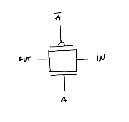
Transmission gates are a bidirectional switch made from an nMOS and pMOS transistor in parallel. The nMOS is controlled by the signal, and the pMOS is controlled by the inverted signal. This switch is good at passing both 0s and 1s.
Noise Margins
The high noise margin is the amount of noise that can be added to a high signal before it is interpreted as a low signal.
The low noise margin is the amount of noise that can be added to a low signal before it is interpreted as a high signal.
The unity gain point is where the slope is equal to 1. That is where and should be set.

Combinational Circuits
A logic circuit is composed of:
- Inputs
- Outputs
- Functional specification
- Timing specification
In a combinatorial circuit:
- Every node is either an input or connects to exactly one output
- There are no cyclic paths
Combinational circuits are memoryless, meaning that the output is solely determined by the input. They are different from sequential circuits, which have memory and whose output is determined by both the input and the current state.
Boolean Algebra
A complement is the inverse of a variable, a literal is a variable or its complement, and an implicant is a product of literals.
| Term | Definition | Example |
|---|---|---|
| Literal | Variable or its complement | |
| Complement | Inverse of a variable | |
| Implicant | Product of literals | |
| Minterm | Implicant that includes all input variables | |
| Maxterm | Sum that includes all input variables |
Sum-of-products (SOP)
- Find the inputs where
- Convert the inputs to minterms
- Sum the minterms
e.g.
| Minterm | Y | ||
|---|---|---|---|
| 0 | 0 | 0 | |
| 0 | 1 | 1 | |
| 1 | 0 | 0 | |
| 1 | 1 | 1 |
Product-of-sums (POS)
- Find the inputs where
- Convert the inputs to reversed maxterms
- Multiply the maxterms
e.g.
| Reversed Maxterm | Y | ||
|---|---|---|---|
| 0 | 0 | 0 | |
| 0 | 1 | 1 | |
| 1 | 0 | 0 | |
| 1 | 1 | 1 |
X is used to indicate:
- Uninitialized values
- Don't care
- Contention (circuit tries to drive output to both 0 and 1)
Bubble-Pushing
Using De Morgan's laws, we can push bubbles through AND and OR gates to change the gate type.
Heuristics:
- Begin at the output and work toward the input
- Draw gates so that bubbles cancel
Tri-State Buffers
A tri-state buffer has 2 inputs (A and EN) and 1 output (Y). Z represents high impedance. The circuit is not driving the output to any logic level.
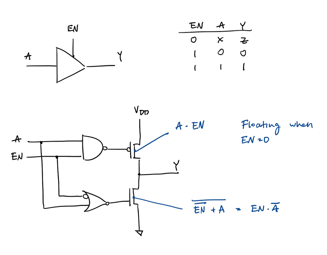
Tri-state buffers are used in busses where there are many different drivers, but only one should be active at a time.
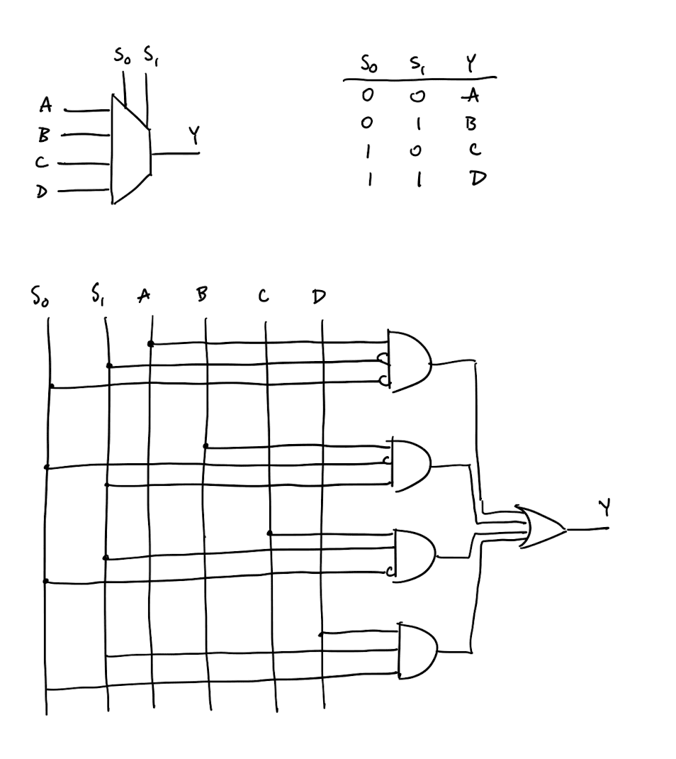
Multiplexers
A multiplexer (MUX) takes in inputs, select lines, and 1 output. The output is equal to one of the inputs, determined by the select lines.
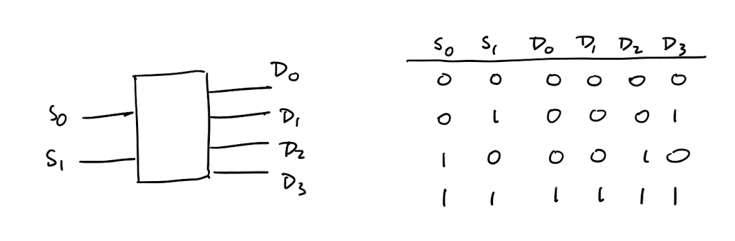
Decoders
A decoder takes in inputs and produces outputs. Only one output is high at a time, determined by the input value. This is called a one-hot output.
Sequential Circuits
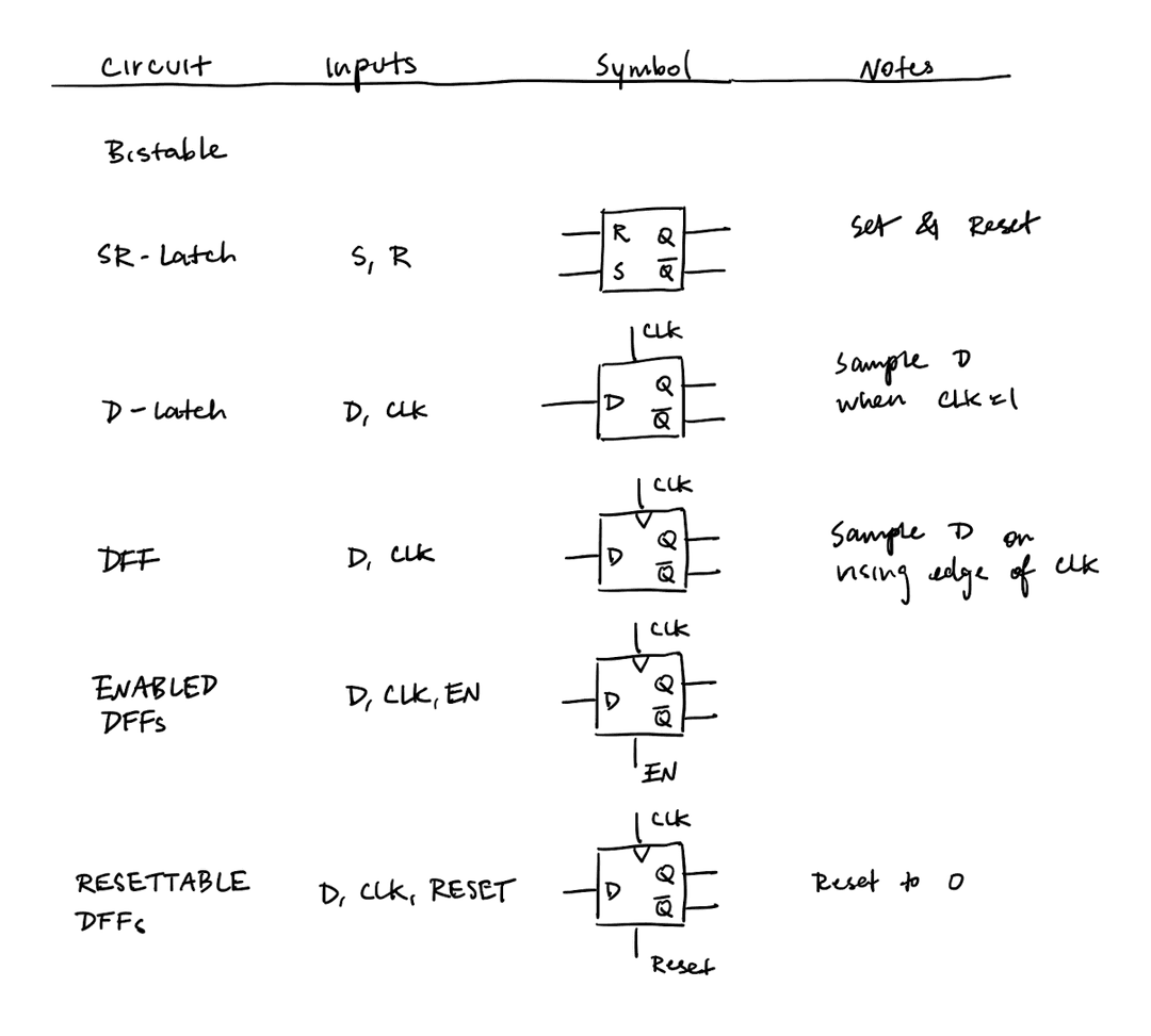
Bistable Circuit
- No inputs
- Stable at two values
- 4 transistors

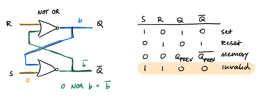
Set-Reset Latch
- 2 inputs (S and R)
- At S = R = 1, we get an invalid state Q = Q' = 0
- 8 transistors
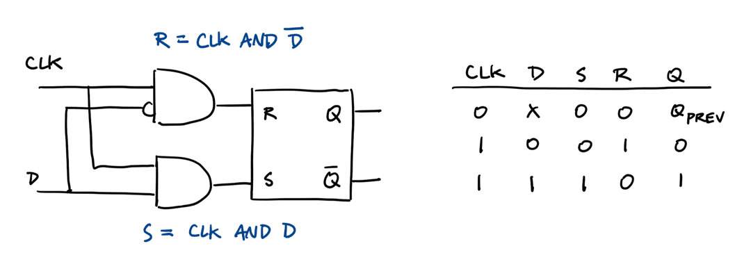
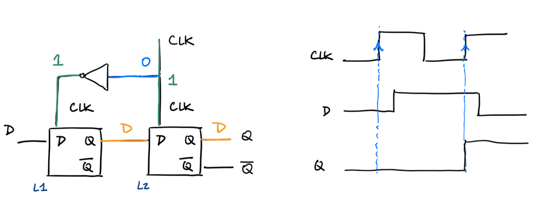
Data Latch
- 2 inputs (CLK and D)
- CLK controls whether the output changes in response to the D
- Avoids the invalid state of the SR latch
- 22 transistors
Data Flip-Flop
- 2 inputs (CLK and D)
- D is sampled on the rising edge of CLK
- Signals start with unknown state
- 46 transistors
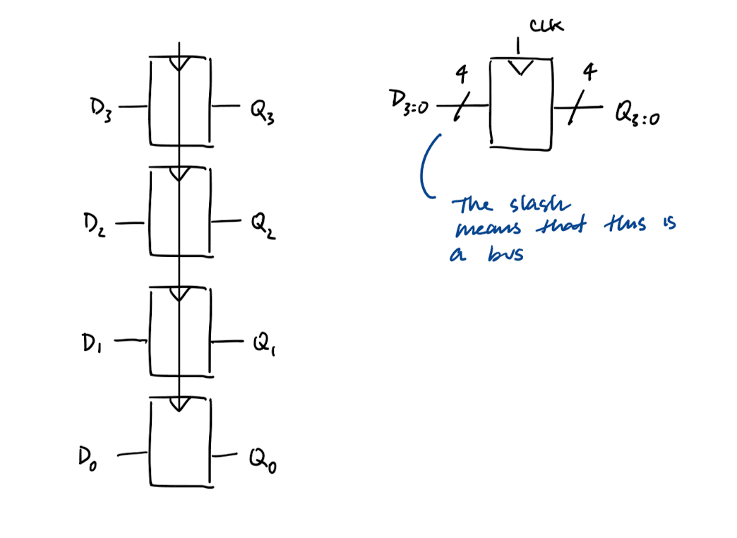
Registers
Registers are made from multiple flip-flops.
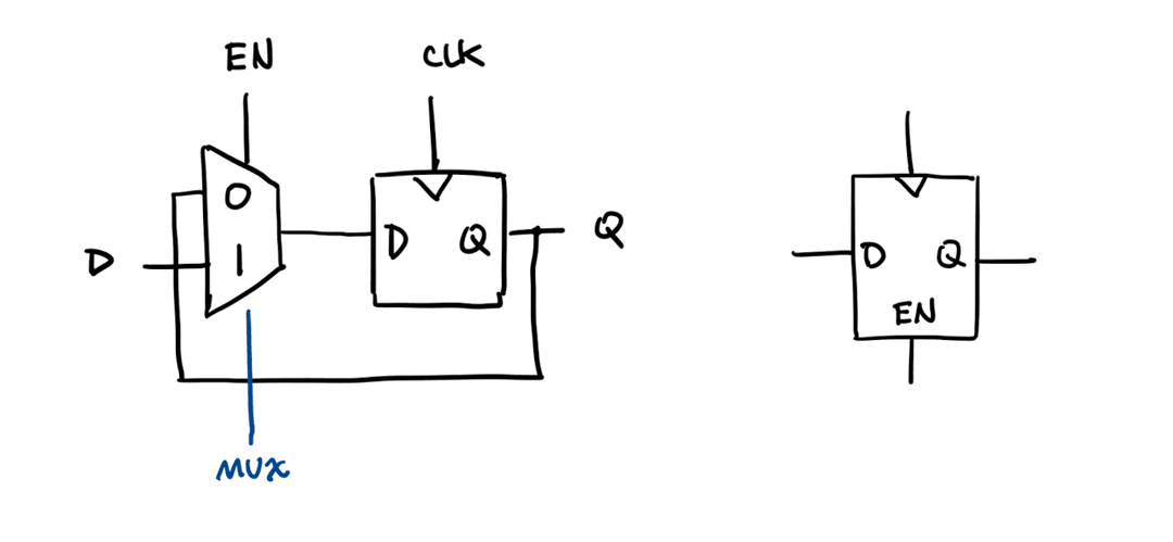
Enabled Flip-Flops
- 3 inputs (CLK, D, and EN)
- The EN controls whether new data is stored
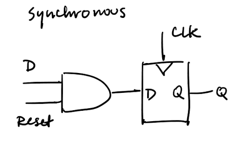
Resettable Flip-Flops
- 3 inputs (CLK, D, and Reset)
- Reset changes Q to initial state 0
Synchronous reset:
- Reset on clock edge
- Easier, just AND
- Timing is consistent
Asynchronous reset:
- Reset immediately when Reset = 1
- Need to change internal circuitry
- Timing is hard
Settable Flip-Flops
- 3 inputs (CLK, D, and Set)
- Set changes Q to state 1
Summary
Synchronous sequential circuits
There are two common types osf synchronous sequential circuits:
- Pipelines
- Finite state machines (FSMs)
Finite State Machines
There are two types of FSMs:
- Moore: Output depends only on current state
- Mealy: Output depends on current state and input
Design procedure:
- Identify inputs and outputs
- Select state encodings
- Sketch a state transition diagram. Nodes represent states and edges represent inputs.
- Write a state transition table and output table
- Write boolean equations for next state and output logic
Verilog
Built-In Gates
For built-in gates, the first terminal in the list of terminals is an output and the other terminals are inputs.
// 1-bit full adder
module FA(a, b, cin, s, cout);
input a, b, cin;
output s, cout;
wire t1, c1, c2;

xor g1(t1, a, b);
xor g2(s, t1, cin);
and g3(c1, t1, cin);
and g4(c2, a, b);
or g5(cout, c1, c2);
endmodule
Buses
Buses are declared with the [n:m] syntax, where n is the most significant bit and m is the least significant bit.
// 4-bit full-adder
module fulladd4(A, B, Cin, S, Cout);
input [3:0] A, B;
input Cin;
output [3:0] S;
output Cout;
wire C1, C2, C3;

FA f1(A[0], B[0], Cin, S[0], C1);
FA f2(A[1], B[1], C1, S[1], C2);
FA f3(A[2], B[2], C2, S[2], C3);
FA f4(A[3], B[3], C3, S[3], Cout);
endmodule
Assign Statements
assign statements can be used to create combinational logic without instantiating gates. Supported operations include arithmetic, logic, relational, bitwise, and ternary.
Note that the left-hand side cannot appear in more than one assign or gate output statement.
module fulladd4(A, B, S);
input [3:0] A, B;
output [3:0] S;
assign S = A+B;
endmodule
Concatenation and replication can be done with the {} syntax.
// concatenation
wire [7:0] busA, busB;
wire [15:0] busC;
assign busC = {busA, busB};
// replication
wire [3:0] a;
wire [11:0] c;
assign c = {3{a}};
Always Blocks
The always block executes whenever a signal in the sensitivity list changes. Multiple statements are grouped in a begin and end block.
Rules:
- Control flow like if-else, case, and looping are only allowed inside always blocks.
- Variables assigned within an
alwaysblock must be declared asregorinteger. - The same variable can be assigned multiple times in an always block. The last assignment takes precendence.
- Use
posedgeornegedgeto trigger on clock edges.
always can model combinational or sequential logic.
- Use
always @(*)and blocking assignments (=) to model combinational logic - Use
always @(posedge clk)and non-blocking assignments (<=) to model sequential elements - Avoid mixing blocking and non-blocking assignments in the same always block
// d-latch
reg c;
  always @clock
    if (clock) c = a + b;
// data flip-flop
reg c;
always @(posedge clock)
    c <= a + b;
// finite state machine
module fsm(clk, inp, out);
input clk, inp;
output out;
wire sig;
reg [1:0] state, next_state;

parameter S1 = 0, S2 = 1, S3 = 2, S4 = 3;
initial state = S1;

assign sig = state[0] & state[1];
not a1(out, sig);

always @(posedge clock)
  case(state)
  S1: state <= inp ? S2:S1;
  S2: state <= inp ? S3:S1;
  S3: state <= inp ? S4:S2;
  S4: state <= inp ? S3:S4;
  endcase
endmodule
Tips
- The simulator might complain if the code doesn't match any of its templates for asyncrhonous reset. [1]
Timing
Physical Reasons for Delay
- Gate delay is impacted by gate type, size, load, and temperature
- Wire delay is impacted by length, fanout, and load of wire
Note that the gate delay when switching from LOW to HIGH is not necessarily the same as the delay when switching from HIGH to LOW.
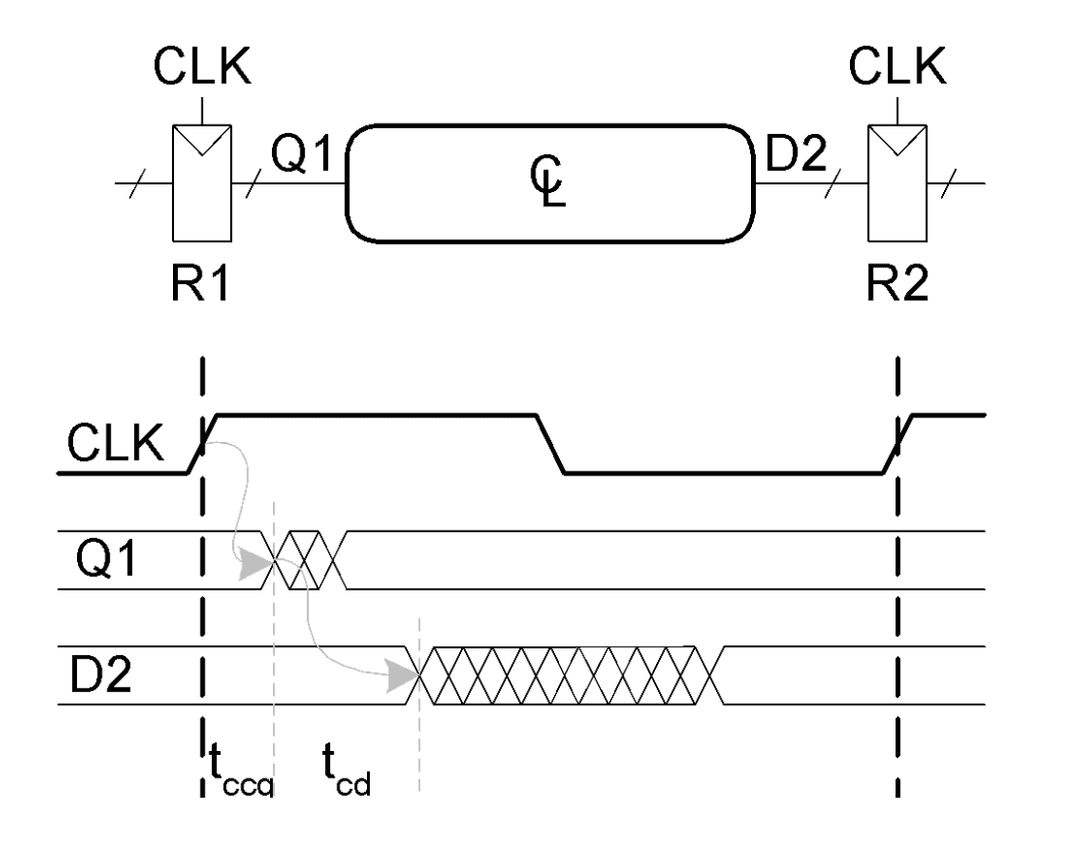
Propagation and Contamination Delay
Propagation delay is the max delay from input to output. Contamination delay is the min delay from input to output.
The critical path is the longest path through a circuit and is associated with . The short path is the shortest path through a circuit and is associated with .
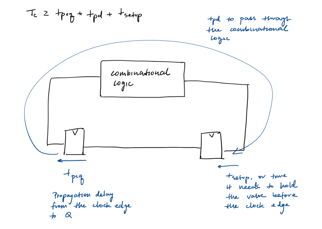
Flip-Flop Delays
For flip-flops, we care about the delay between the clock and the output, not the delay between the input and the output.
The propagation delay is the time after the clock edge that Q is guaranteed to be stable; i.e. max delay The contamination delay is the time after the clock edge that Q may start changing; i.e. min delay.
The setup time is the time before the clock edge where data must be stable. The hold time is the time after the clock edge where data must be stable. Finally, the aperture time is the time around the clock edge where data must be stable. .
The setup time is really the propagation time through the first data latch in the flip-flop. The hold time is the propagation time from the CLK to the first data latch.
Combinational Delays
The delay between registers have a minimum and maximum delay due to combinational logic.
The setup time constraint requires that . Usually is a design constraint, and is given, and we want to optimize in the combinational logic.

Some ways to fix setup time violations include:
- Restructuring the combinational logic
- Inserting buffers on long wires
- Minimizing wirelength
- Increase the clock period and take the hit
The hold time constraint requires that . Usually and are given, and we want to optimize in the combinational logic.
Some ways to fix setup time violations include:
- Adding delay buffers on short paths
- Increasing the length of short wires
Hold time violations can cause glitches, wasting power.
Static Timing Analysis
Static timing analysis (STA) is a method to determine if a circuit meets timing constraints without simulating all possible input combinations.
Clock Skew
When the clock arrives at different flip-flops at different times, this is called clock skew. Skew eats from both our setup time and hold time budget.
Synchronizers
Asynchronous inputs can create timing violations.
Synchronizers are used to safely transfer signals between different clock domains. A common synchronizer is a chain of two flip-flops.
Digital Components
Memory Arrays
Memory arrays are used to store large amounts of data.

Appendix
Powers of 2
| n | 2^n |
|---|---|
| 0 | 1 |
| 1 | 2 |
| 2 | 4 |
| 3 | 8 |
| 4 | 16 |
| 5 | 32 |
| 6 | 64 |
| 7 | 128 |
| 8 | 256 |
| 9 | 512 |
| 10 | 1024 |
| 11 | 2048 |
| 12 | 4096 |
Large powers of 2
| n | 2^n |
|---|---|
| 10 | 1K (10^3) |
| 20 | 1M (10^6) |
| 30 | 1G (10^9) |
| 40 | 1T (10^12) |
| 50 | 1P (10^15) |
| 60 | 1E (10^18) |
For example, 2^32 = 2^2 * 2^30 = 4 billion.